
This semester at ITP I'm taking a class called Homemade Hardware. This class was a last-minute addition to my schedule after I started talking with Solid Wiggles about a possible collaboration (see my previous post). In order to take DJELLO to the next level, I realized I would need to make my hardware more durable and potentially mass-producible. One solution to this is to design and produce PCBs - printed circuit boards. PCBs are probably what you picture when you hear the phrase "circuit board".
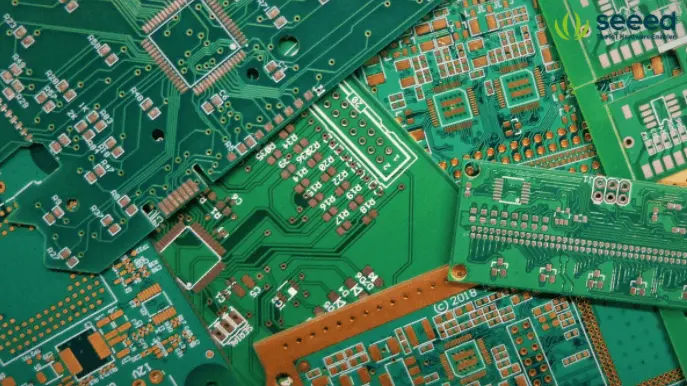 Some examples of PCBs
These boards let you create permanent circuits, as opposed to the temporary circuits made on breadboards. During our first semester at ITP, all students were given a breadboard so that we could experiment and prototype circuits without having to solder anything. Breadboards have lots of electrically connected holes that you can plug wires, microcontrollers, and other components into. For example, here was my breadboard for DJELLO's sensors. There's tons of wires that could very easily come unplugged -- it's a mess.
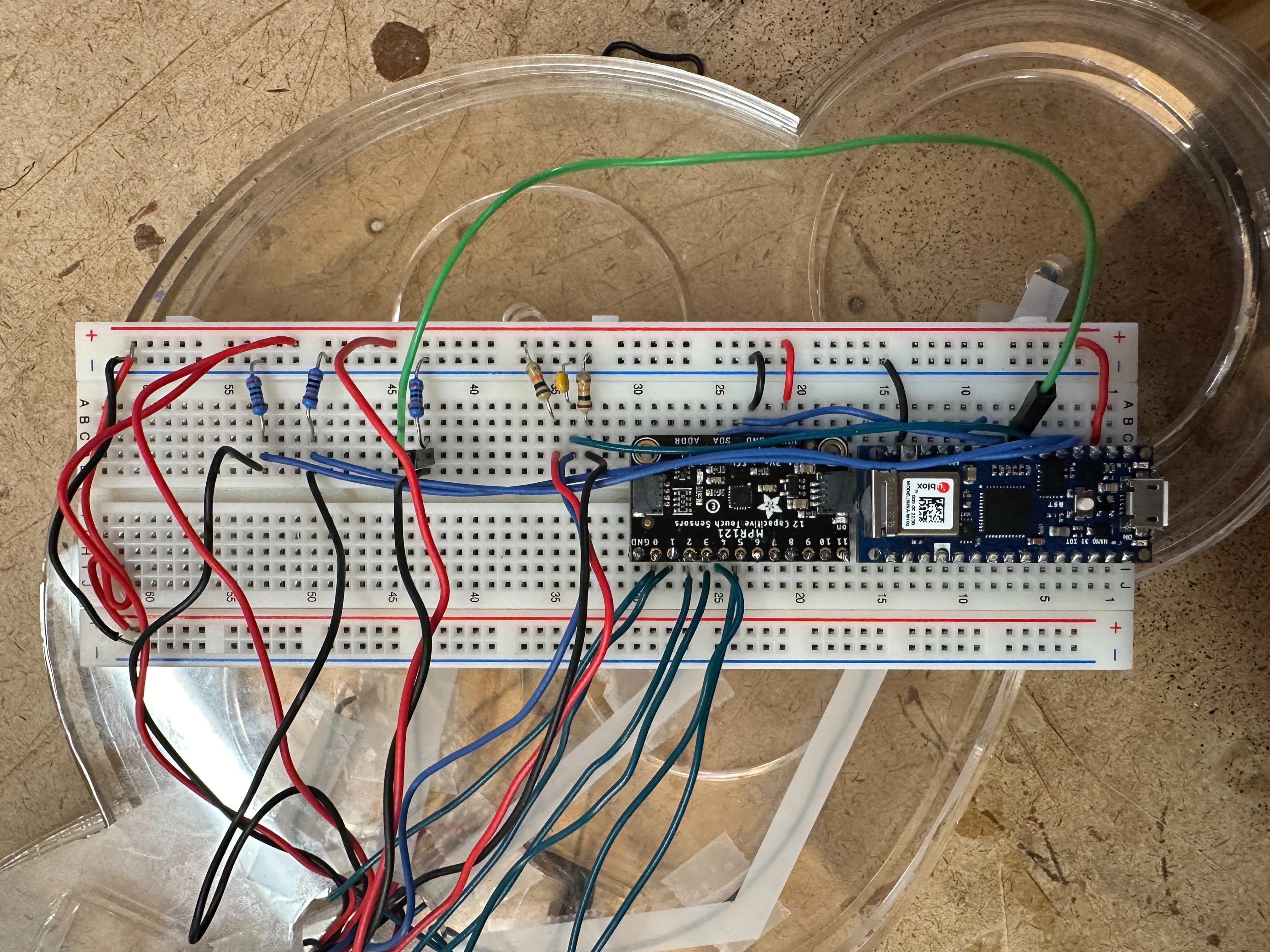 My breadboarded circuit for DJELLO to connect multiple sensors
This isn't something that I can easily transport, reproduce, or debug if I wanted to use it at an event with Solid Wiggles. My goal for Homemade Hardware is to create a PCB that will make all of this permanent. A small board that you can plug in to a piece of Jello and will play a sound if the Jello is being touched. I'll be working on this soon for the final project. Up until now I've been working on the midterm project to get familiar with the process of designing, fabricating, and programming a PCB.
The midterm project was to create a PCB to serve as one letter in a class marquee sign -- one of those signs where each letter is illuminated with several lights. The class nominated the phrase "START CRYING" for the marquee sign and I was assigned to make the letter N.
Board Design
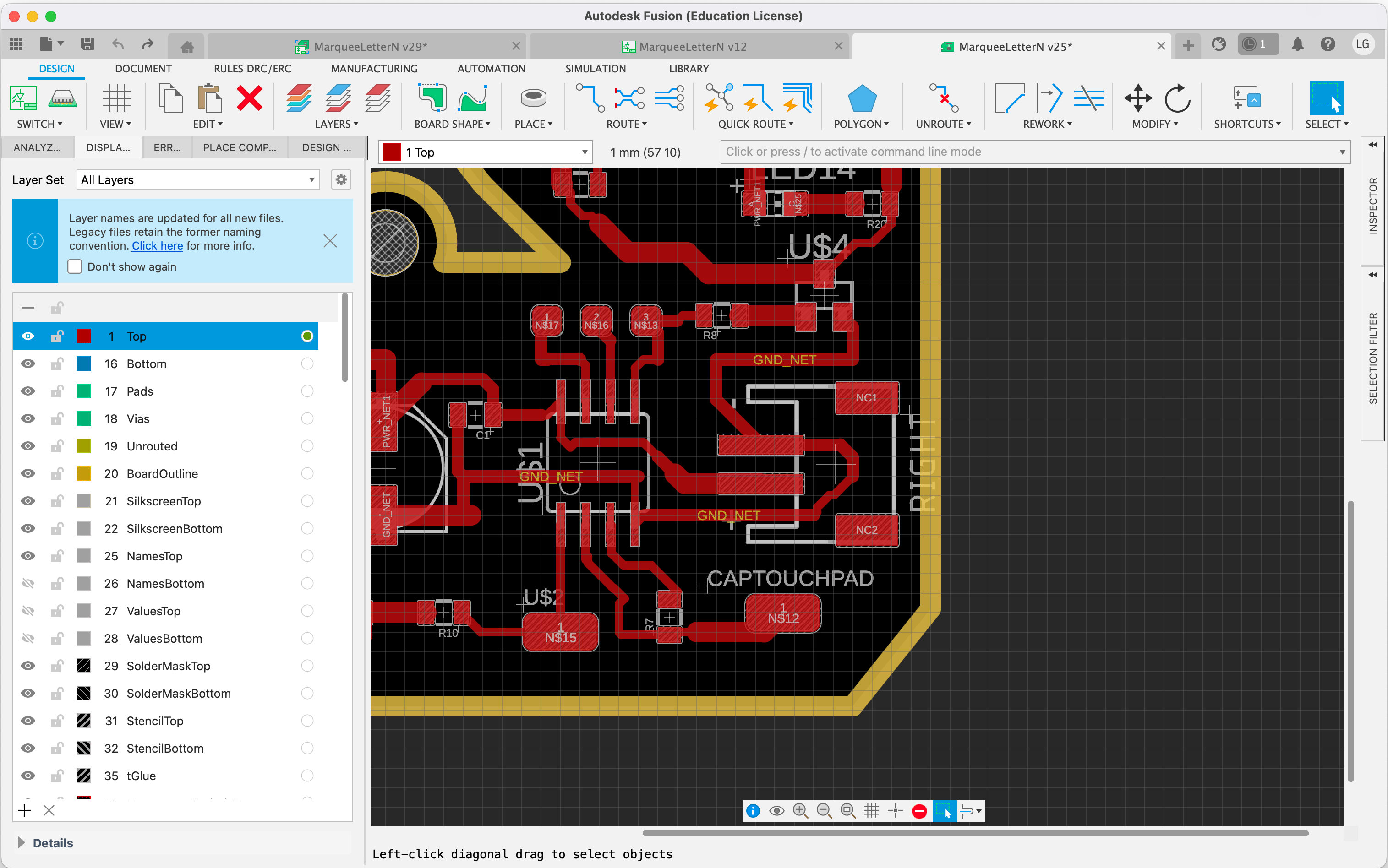
Before physically building anything, the first step is to design the circuit. I used Autodesk Fusion 360 to create the circuit schematic and map that onto a physical board layout. The schematic lets you build a digital circuit so you can specify what components are connected to power, ground, other components, etc. The key component in this circuit is an ATTiny, a very small microcontroller that is the brains of the board. This chip is used in place of an Arduino, which is much larger and has more input pins than this circuit needs.
 An Arduino Nano (on top) compared to the ATTiny (small black box on the bottom)
Here is most of my schematic. The full schematic is too large to include here because it has a huge row of 22 LEDs to form the letter N out of lights, you can see the start of this row on the top right of the diagram. But most of the interesting stuff is included here: the ATTiny, power and ground lines, a capacitive touch sensor to make the lights interactive, and a transistor to let us control lots of LEDs from one microcontroller pin. This schematic tells what components are in this circuit and how they are connected, but it doesn't tell us how they are physically organized on a real board.
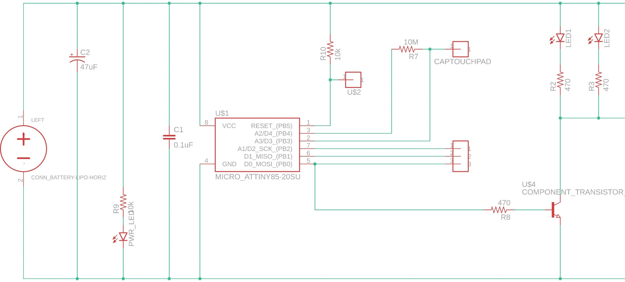 The PCB's circuit schematic
This schematic can be used to make a board layout. In board layout mode we can see the physical shape of each component from the schematic, so everything is to scale now. This step is all about placing tiny components on the board in the letter N shape while connecting all of them with traces -- the red squiggly lines you see. These lines are essentially 2D wires that will be etched into the board's copper surface. They're all 1mm thick or less! There are constraints on how thick some of the traces can be based on the physical parts and the milling machine bits that I'll explain in the next step.
I had to draw these connections for every component while taking care not to cross any wires. It was sort of a spatial puzzle of untangling a complicated knot, to get every component laid out on a 2D surface while keeping the wires as simple as possible.
 Part of the board layout showing the ATTiny connections
Here's my final board layout. I marked all of the LEDs with green dots since these lights will glow green when the board is programmed and connected to power. The thick yellow outline shows the shape the board will be cut into, which will be the letter N. I'm not very good at spatial visualization so it was difficult to place the LEDs in the shape of an N while letting them all connect to power and ground.
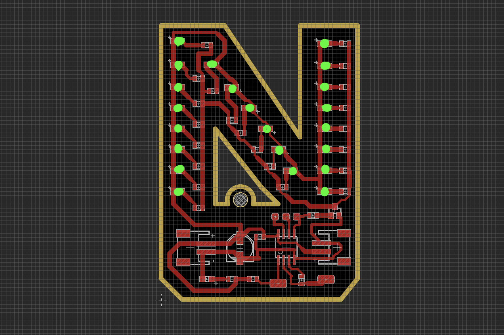 The whole board layout with LEDs on top and the circuit logic on the bottom
Milling
After completing my board design I learned how to use a Bantam milling machine to etch my circuit onto a copper prototype board. These aren't the stereotypical green circuit boards that I mentioned earlier, but super thin pieces of copper glued onto fiberglass. They're insanely cheap so they're good for prototyping. What aren't cheap are the milling bits used in the machine to scrape away pieces of copper and drill through the board. Copper is conductive, so PCBs work by using lines of copper as wires to connect components on the board. The milling machine engraves the circuit by stripping away bits of copper around those wires, so that there's a clear path for electricity to flow as dictated by the board layout. I used a 1/32" and 1/16" bit here.
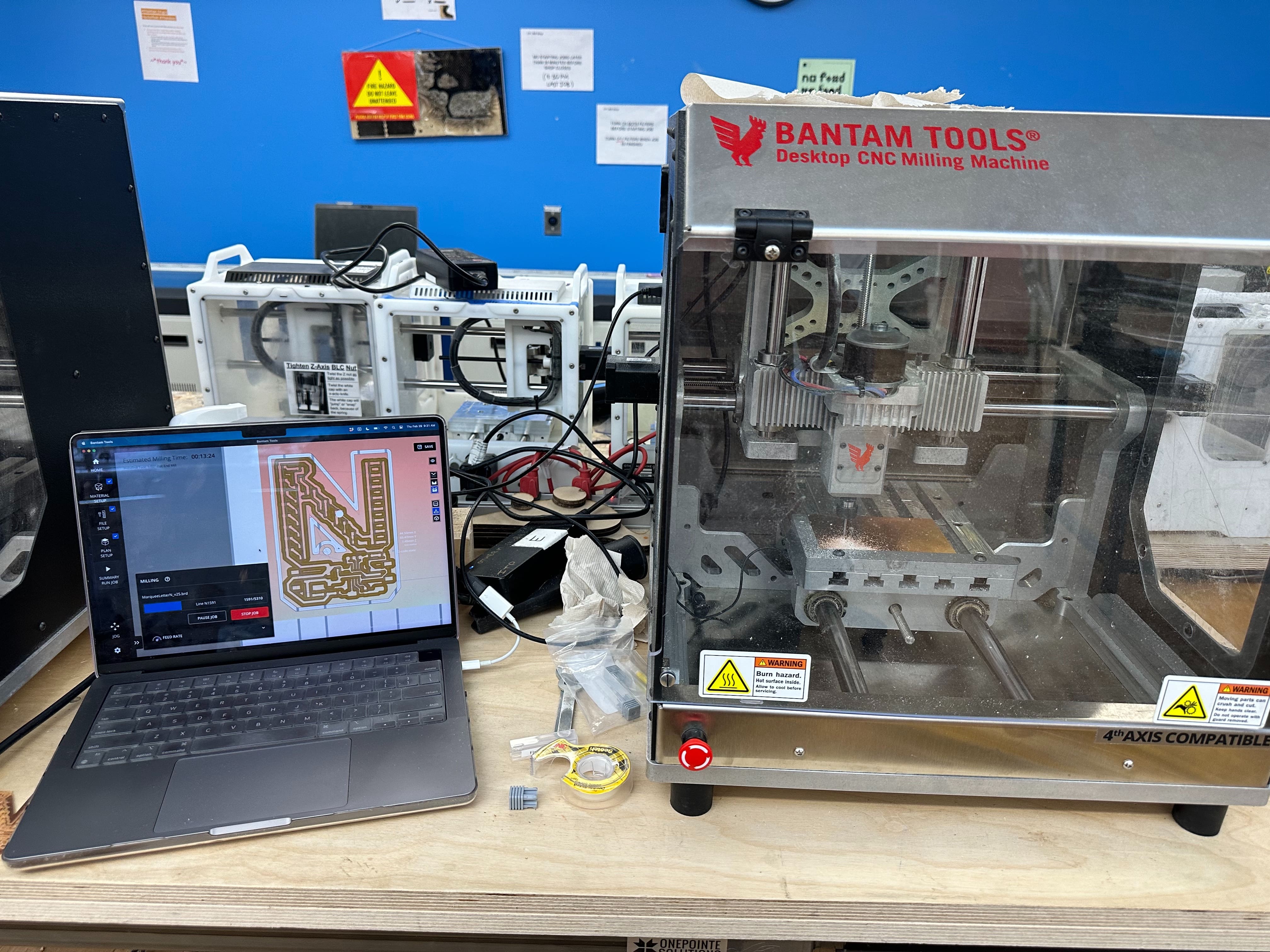 The Bantam milling machine
The Bantam software plans thousands of detailed cuts to make based on my board layout. It's a very precise operation and takes a lot of time to set up to calibrate the material thickness and placement on the machine bed. On my first milling attempt I got the copper board thickness wrong by ~0.1mm, which led my $20 milling bit to break :(
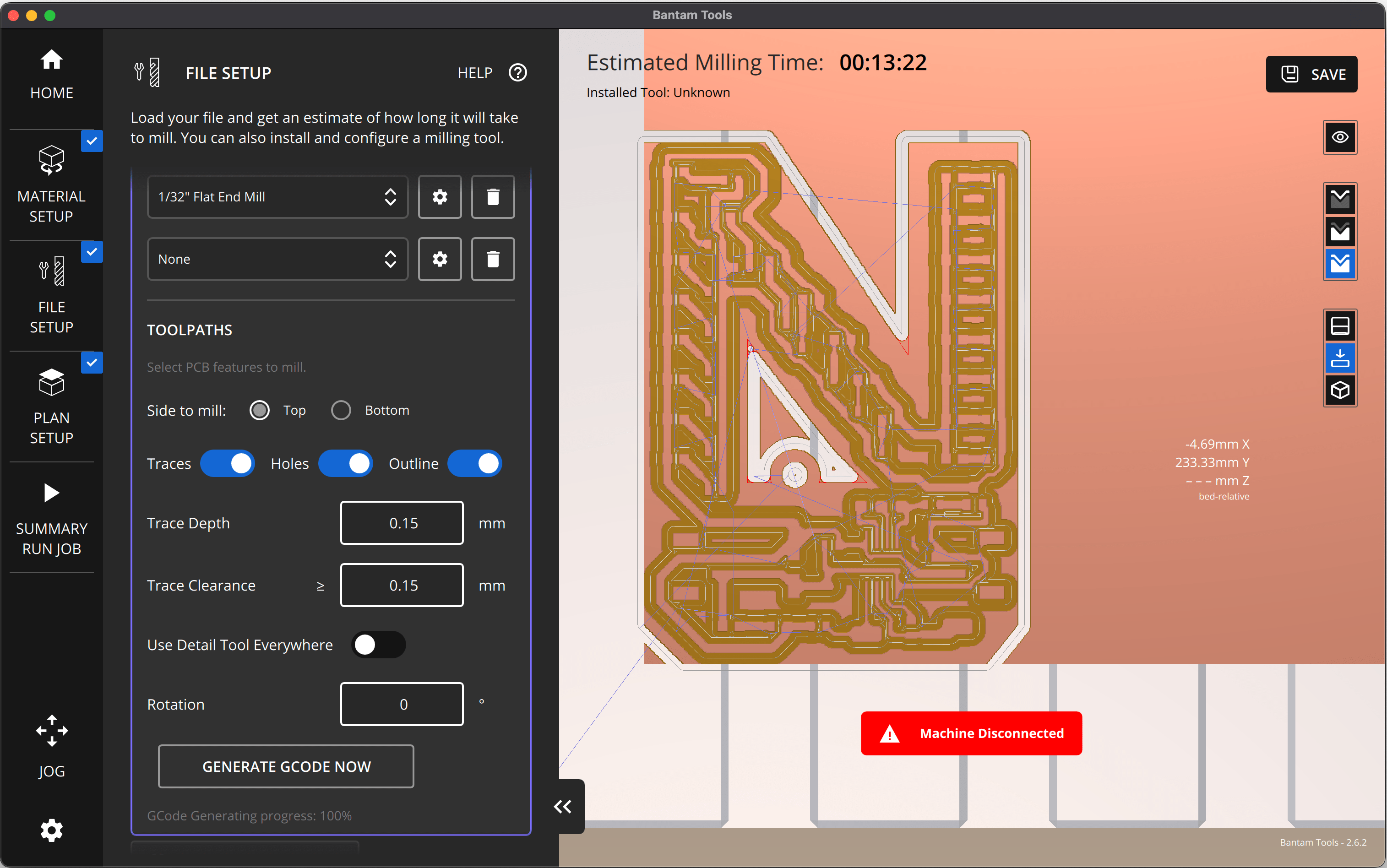 My board layout in the Bantam milling software
Milling my board was insanely stressful because there were so many ways to mess up and I had limited time and resources. It took me 3 attempts to get a correctly milled board. My biggest roadblocks were
- Not measuring the material thickness correctly, causing a bit to go through the board, hit the bed, and break
- Placing my design too close to the edges of the material, causing another bit to hit a metal placement bracket and break
- Getting my board to stick perfectly flat to the bed. I used double-sided tape to secure the board to the bed, and it had to be perfectly flat since the milling bit is scraping off such a thin layer of copper. On my second attempt, the center of the board was slightly higher than the edges, and I calibrated the thickness based on the center. This resulted in the bit not reaching the edges of my board and not engraving that part of the circuit (shown below)
 A failed milling attempt. That big chunk of copper in the bottom left corner should have been engraved, but the bit couldn't reach it
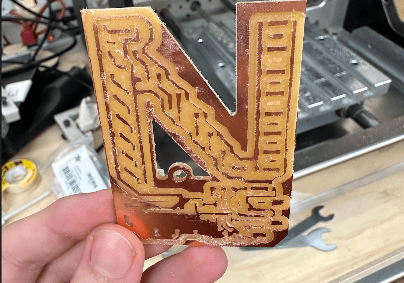
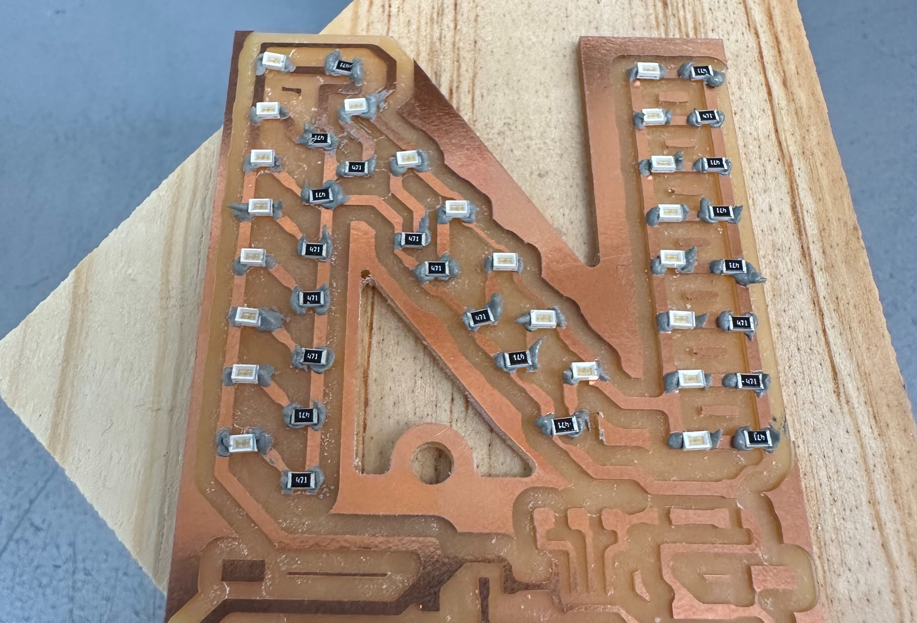
I learned from all of these mistakes and eventually milled a working board! All of the copper traces that I specified in my board layout are there. There's some extra chunks of copper left behind, like on the edges of the letter N shape, because the milling machine only takes away the minimum amount of copper needed to create the circuit. These chunks aren't touching any functional copper traces so they're okay to ignore.
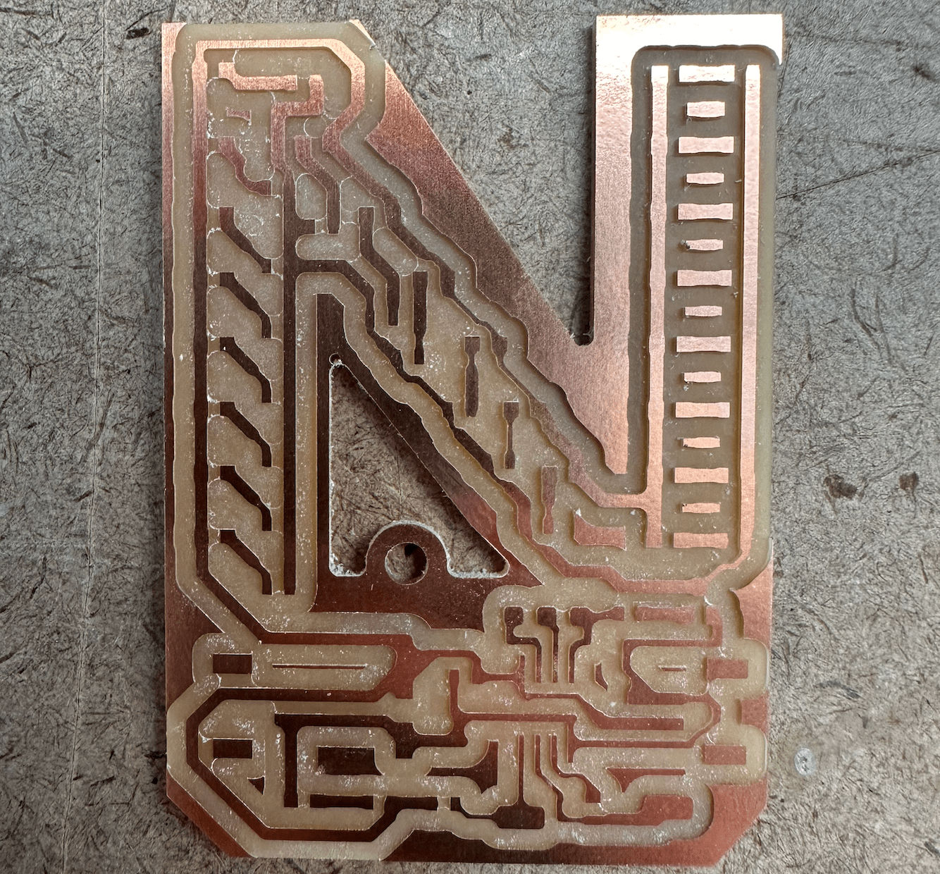 My circuit successfully milled onto the copper board
Assembly
I used a pick and place machine to place tiny surface mount components onto my board. And when I say tiny, I mean TINY. Manipulating these pieces feels like performing brain surgery, it takes a steady hand and good eyesight.
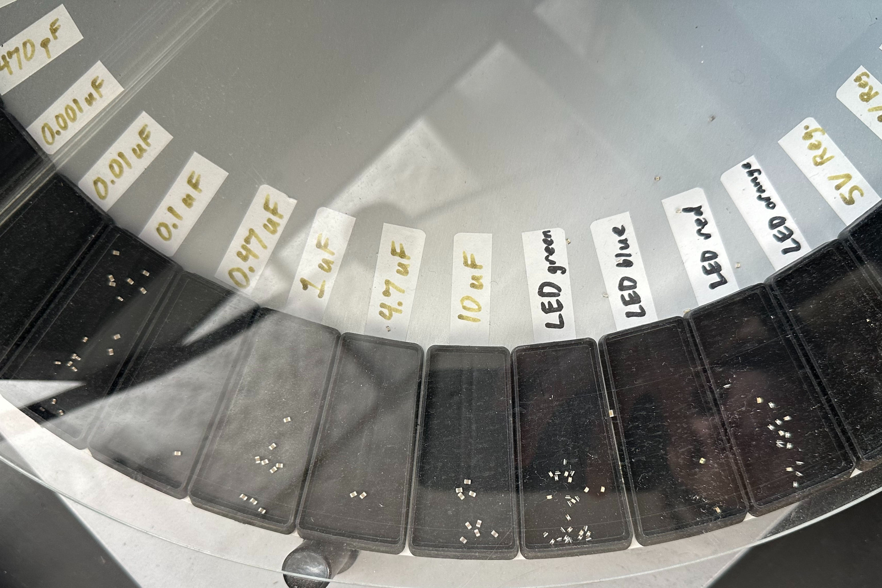 The teeny tiny surface mount LEDs on the tray of the pick and place machine
The pick and place machine reduces the shaky hand problem a bit but still requires concentration. It uses suction to assist in picking up components from the tray and placing them onto the board at precise locations, since we're talking fractions of a millimeter margins of error here. The green nozzle acts like a switch and begins to apply suction when it first taps a component, which makes it pick up the tiny, lightweight piece. It has a movable arm so you can position and rotate the piece over the board. When you lower the nozzle and the suctioned-up piece touches down, the switch triggers again and the suction releases, dropping the piece into place on the board.
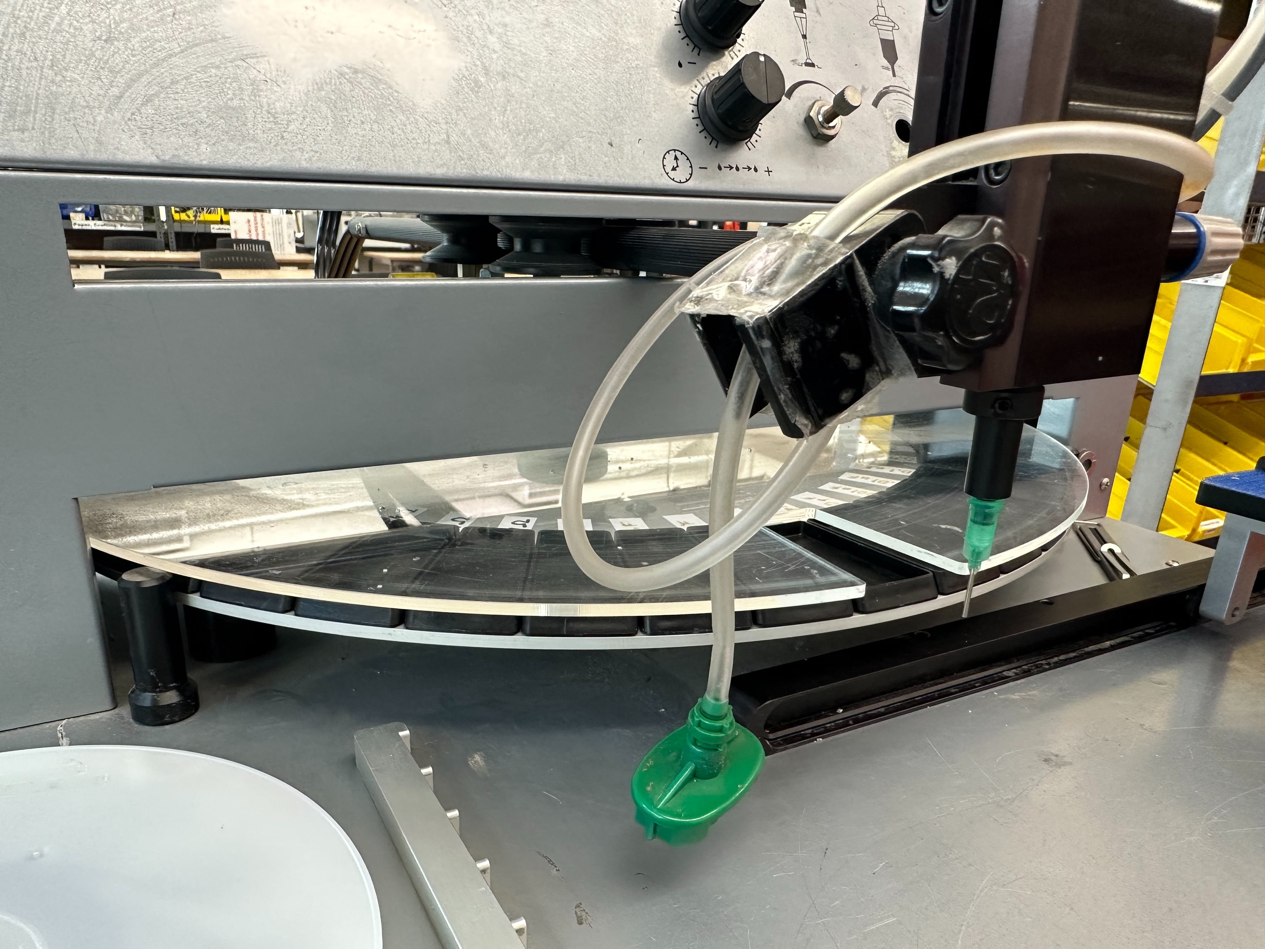 Pick and place machine nozzle (green)
So the process is
- Gather all necessary surface mount components and place onto the tray wheel
- Apply solder paste to the copper board surface where components need to stick, based on the board layout schematic
- Use the pick and place machine to carefully place every component onto the solder paste blobs
- Melt the solder paste to secure the pieces on the board and create electrical connections with the copper
 Placing all the LEDs and their resistors with solder paste
After placing all the components, I had to melt the solder paste to form electrical connections between the components and the copper traces on the board. This process was slightly terrifying because while heating, some air bubbles trapped in the solder expanded and popped, splattering burning hot solder at me. When this happened I went back to the solder paste and pick and place machine to replace the components.
 Gradually heating the board and melting the solder paste on a mug heater
Finally I had a fully assembled board and was ready to test! I connected the board to power and saw that my blue power indicator turned on! And nothing exploded! Both good signs. I also kept my finger on the ATTiny, the black box on the board, to make sure it wasn't overheating, which could indicate an electrical short.
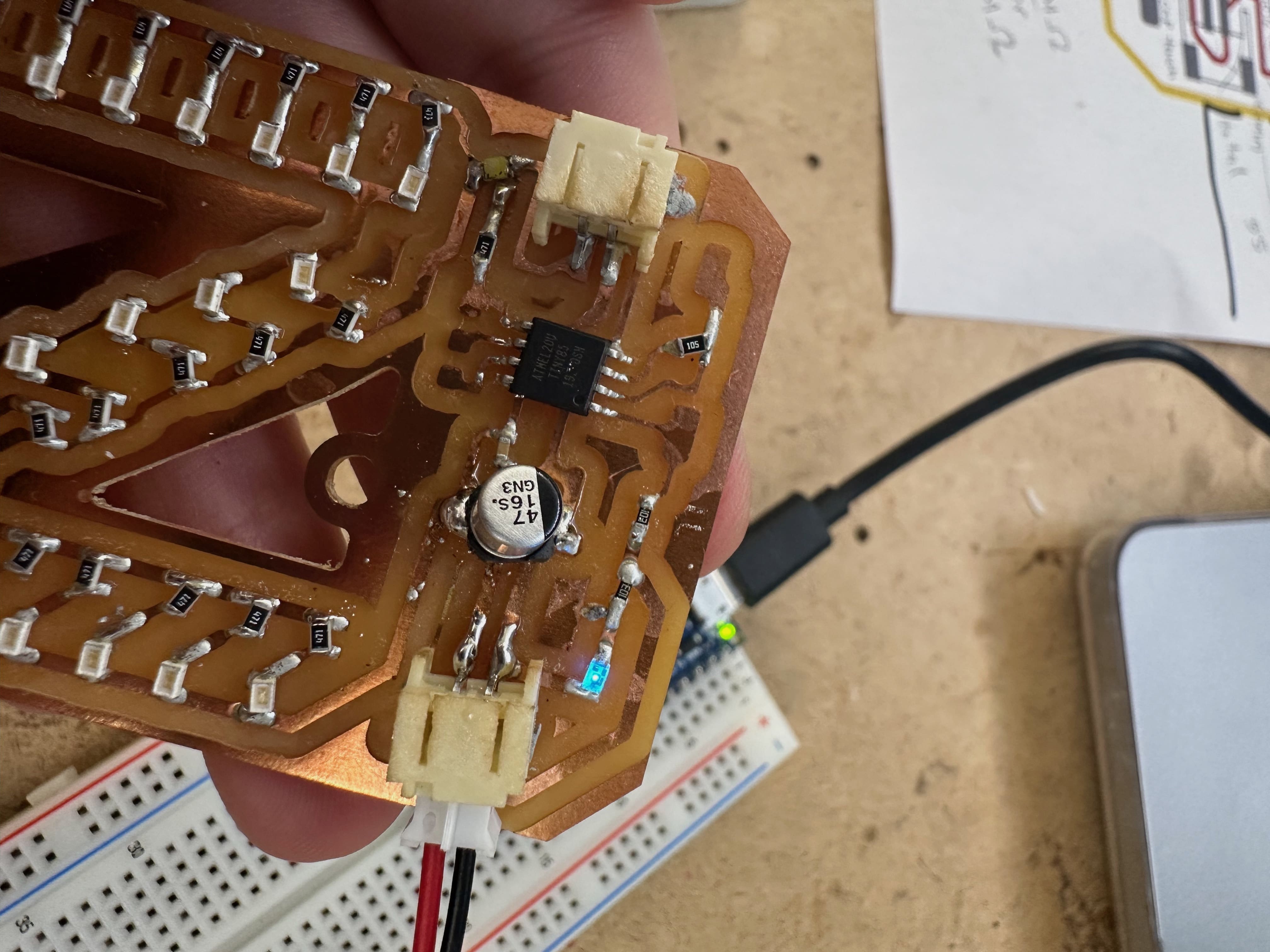 Glowing blue light means the board is receiving power!
Programming
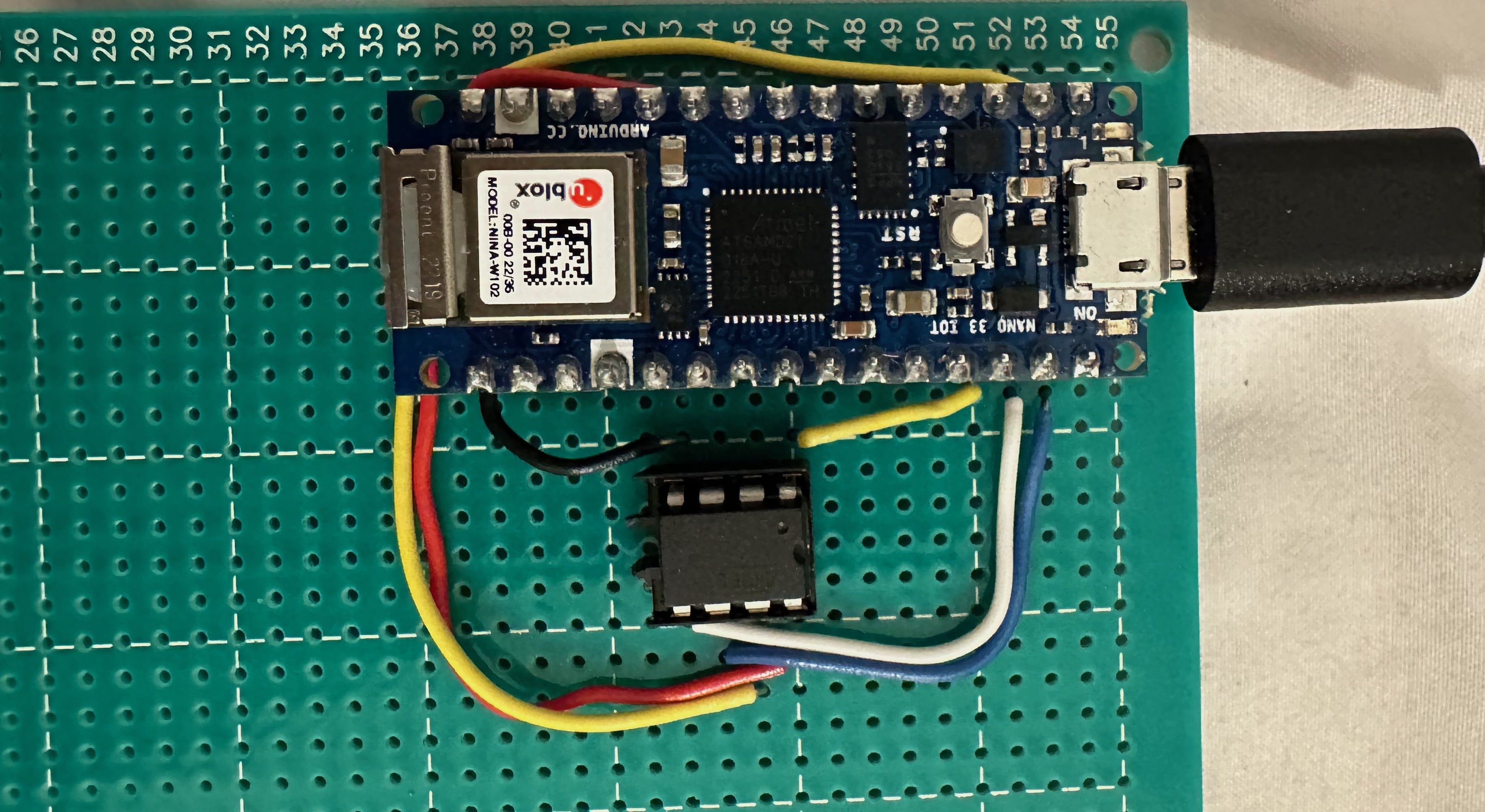
The next step was to program the ATTiny chip. Usually to program an Arduino microcontroller I plug it into my computer via USB and upload code. But the ATTiny doesn't have any kind of port, it just has 8 input/output pins. Two of those pins are used for connecting it to power and ground. Four more pins are used to connect the ATTiny to the larger Arduino chip via wires, which connects to my laptop. This lets me use the Arduino as an intermediary to burn the ATTiny bootloader and upload my code so I can control the lights on the PCB.
So I soldered some programming wires to my ATTiny, and connected the other ends to my Arduino on a breadboard. I had to be very careful to map the correct ATTiny pins to the correct Arduino pins -- each pin has a different purpose in the SPI (serial peripheral interface) protocol and they can't be mixed up. "Peripheral" means the ATTiny is kind of a secondary device being programmed by the primary Arduino.
- Blue wire:
MISO- main in, sub out. Communication line from ATTiny → Arduino - Purple wire:
MOSI- main out, sub in. Communication line from Arduino → ATTiny - Green wire:
SCK- clock. Keeps the Arduino and ATTiny on the same communication rhythm - White wire:
RESET. When re-uploading code, resets the device states to initial values
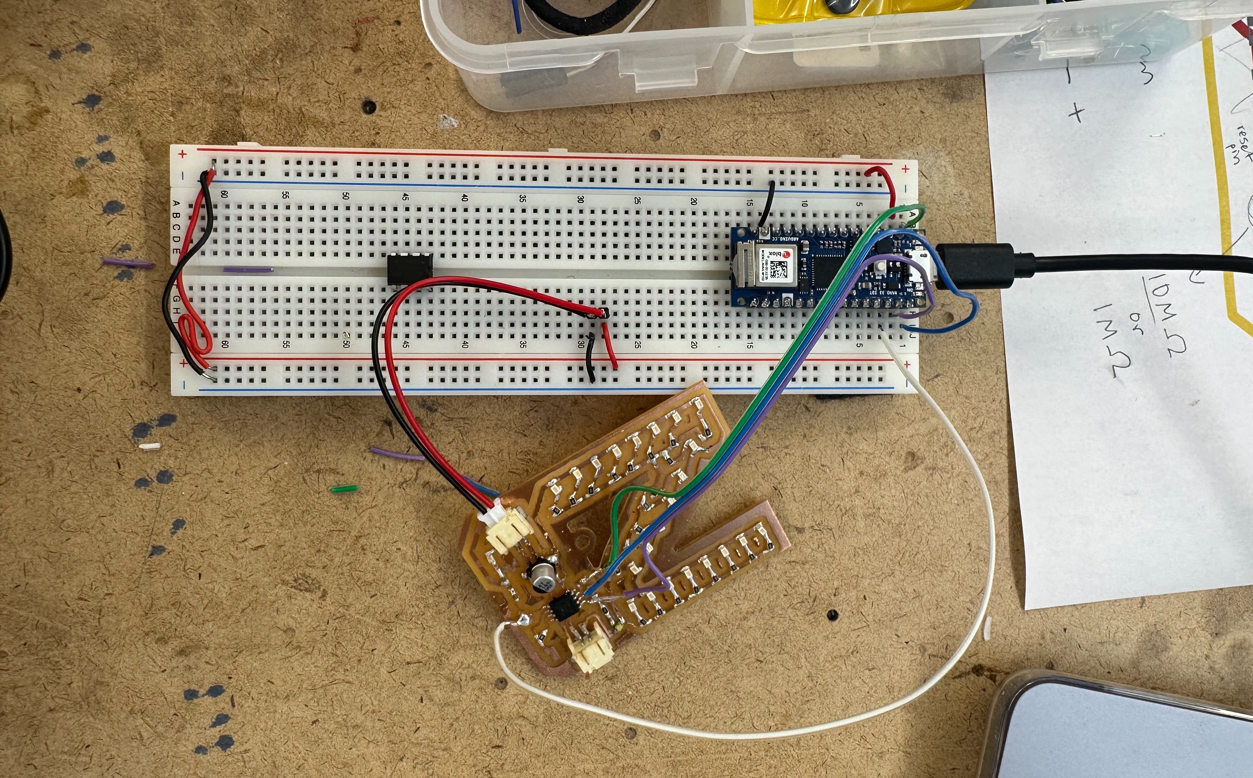 Several programming wires going between my breadboarded Arduino and my board's ATTiny chip
This let me successfully get code running on my PCB letter! But of course I still ran into problems.
Debugging
After uploading code for the first time I expected to see my green LEDs turn on... but nothing happened. I had to play the fun guessing game of whether my software or hardware was broken. Or both. It turned out to be both. After a few hours of debugging here's all the problems that I triaged.
No LEDs turning on
The code I uploaded should have lit up 22 green lights on my board, but they were all off. I immediately suspected something was wrong with the circuit's transistor, which sits between the ATTiny output pin and the LED line. It acts like a gate to provide power to the LEDs. This is necessary to help the microcontroller power 22 LEDs with electrical current from just one pin. No power was reaching the LEDs so I was suspicious of the transistor.
Turns out I was right to be, because the component I had soldered to my board was in fact an LED and not a transistor. It was labeled as a transistor on the pick and place machine tray and I trusted the label blindly, but it was a lie! I had to take this component off of the board and replace it with a real transistor. Taking components off isn't easy because they're soldered to the board pretty securely. I used the tip of a soldering iron and solder wick ribbon to remove chunks of solder, letting me pop off the component.
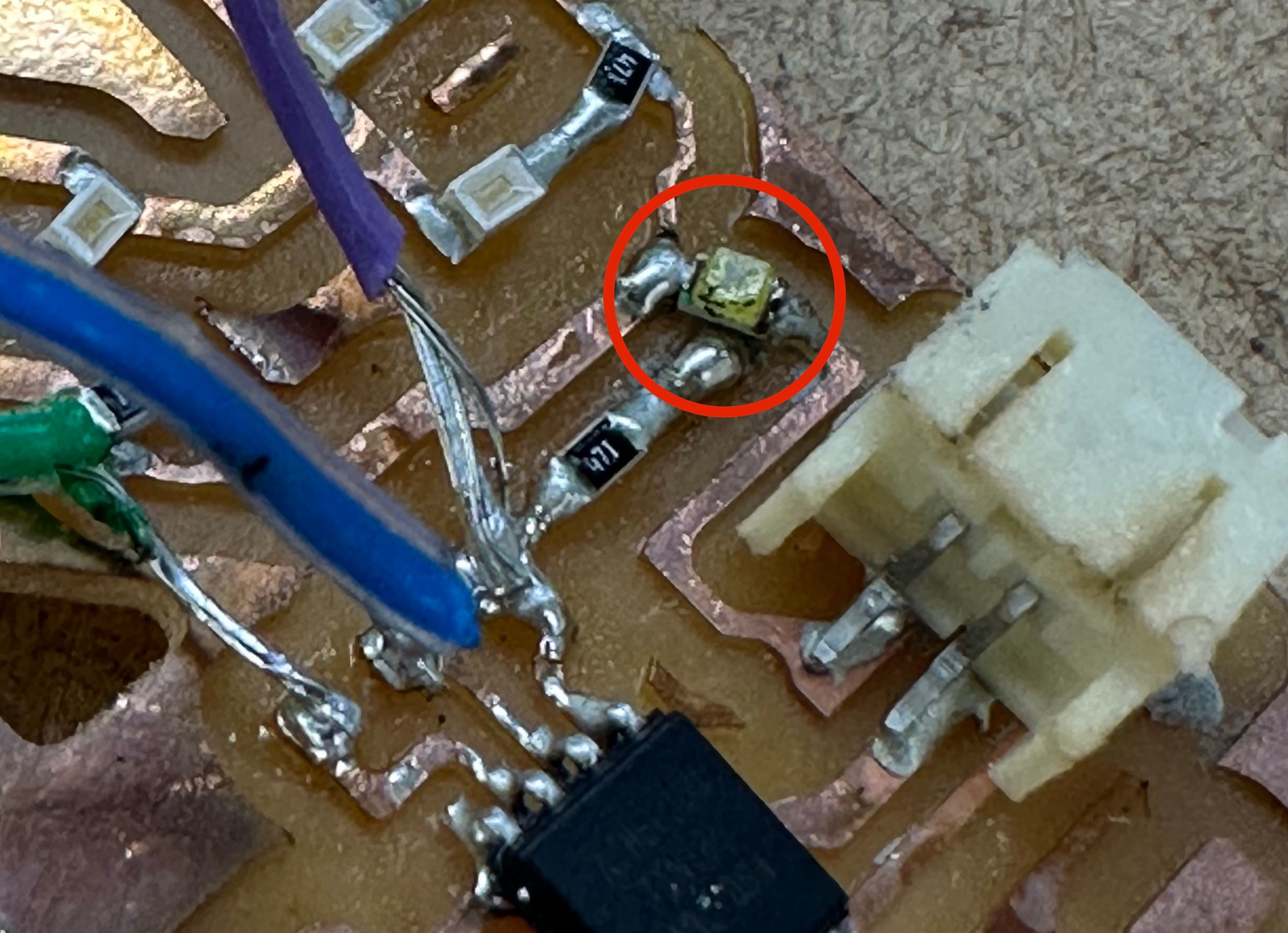 The transistor imposter, an LED
After jumping back to the assembly process to add a transistor, I powered on my board again. This time some of the LEDs turned on -- success!
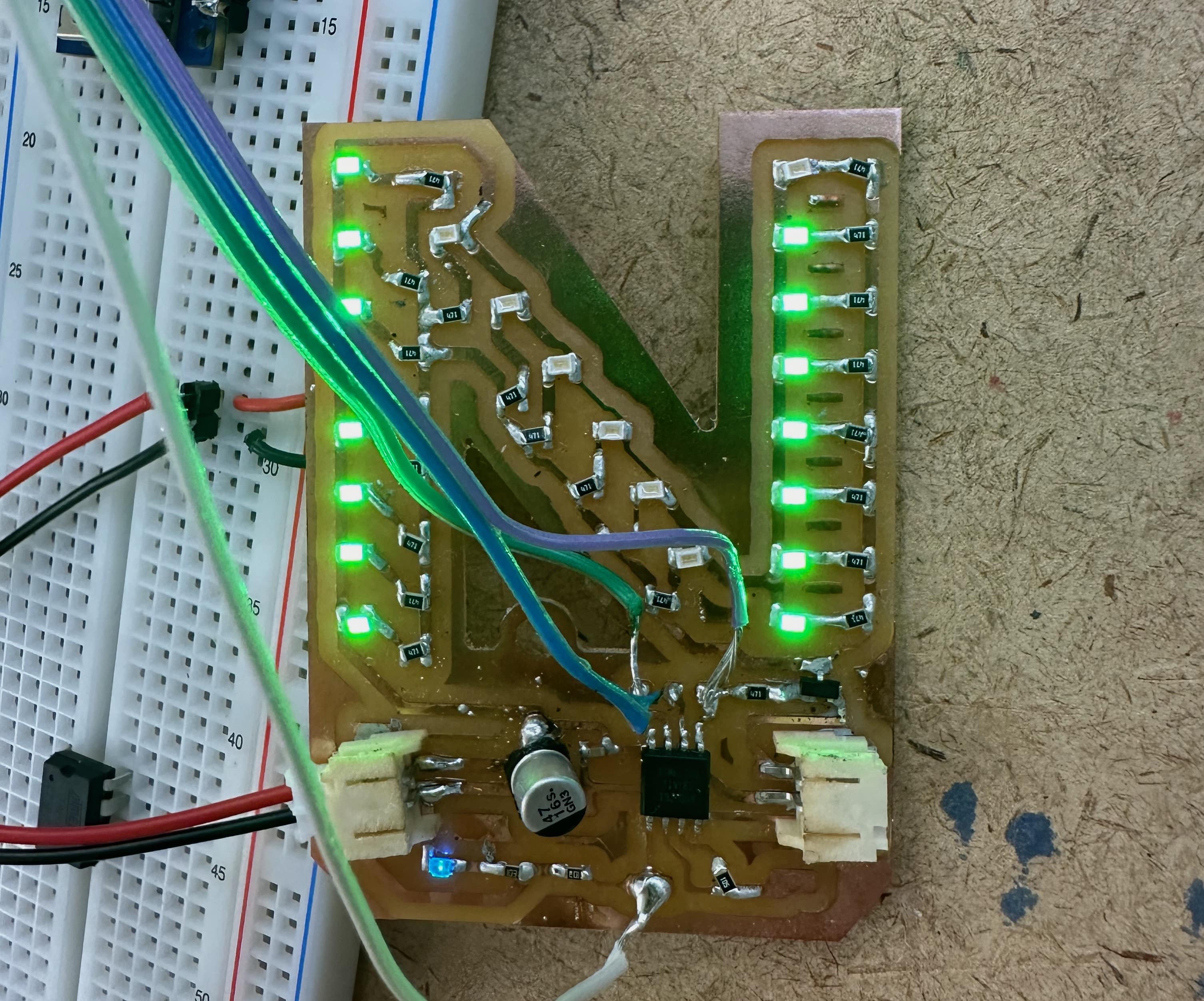 Some green LEDs turned on for the first time, but some still aren't working
Flipped LEDs
Not all of the LEDs were lighting up. I guessed that the non-functional ones were in backwards, because LEDs have a polarity and putting them in backwards can break them. I got a lot more practice in removing components from the board, while being careful not to peel off the thin copper traces along with the solder. Thankfully the LEDs were pretty easy to just break and scrape off, and I could remove excess solder blobs with the soldering iron. I re-assembled the board with new LEDs in the correct orientation, and they all turned on!
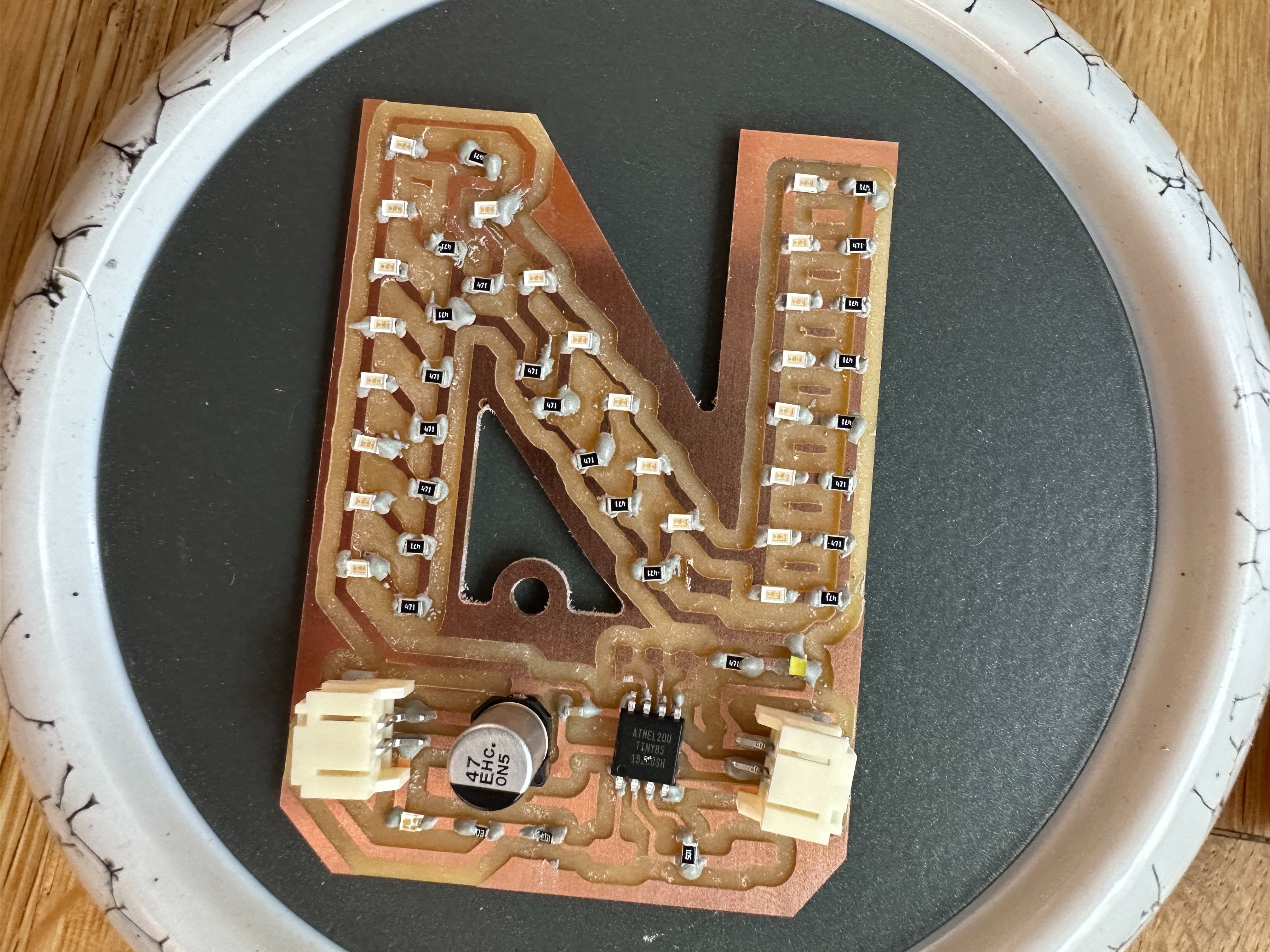
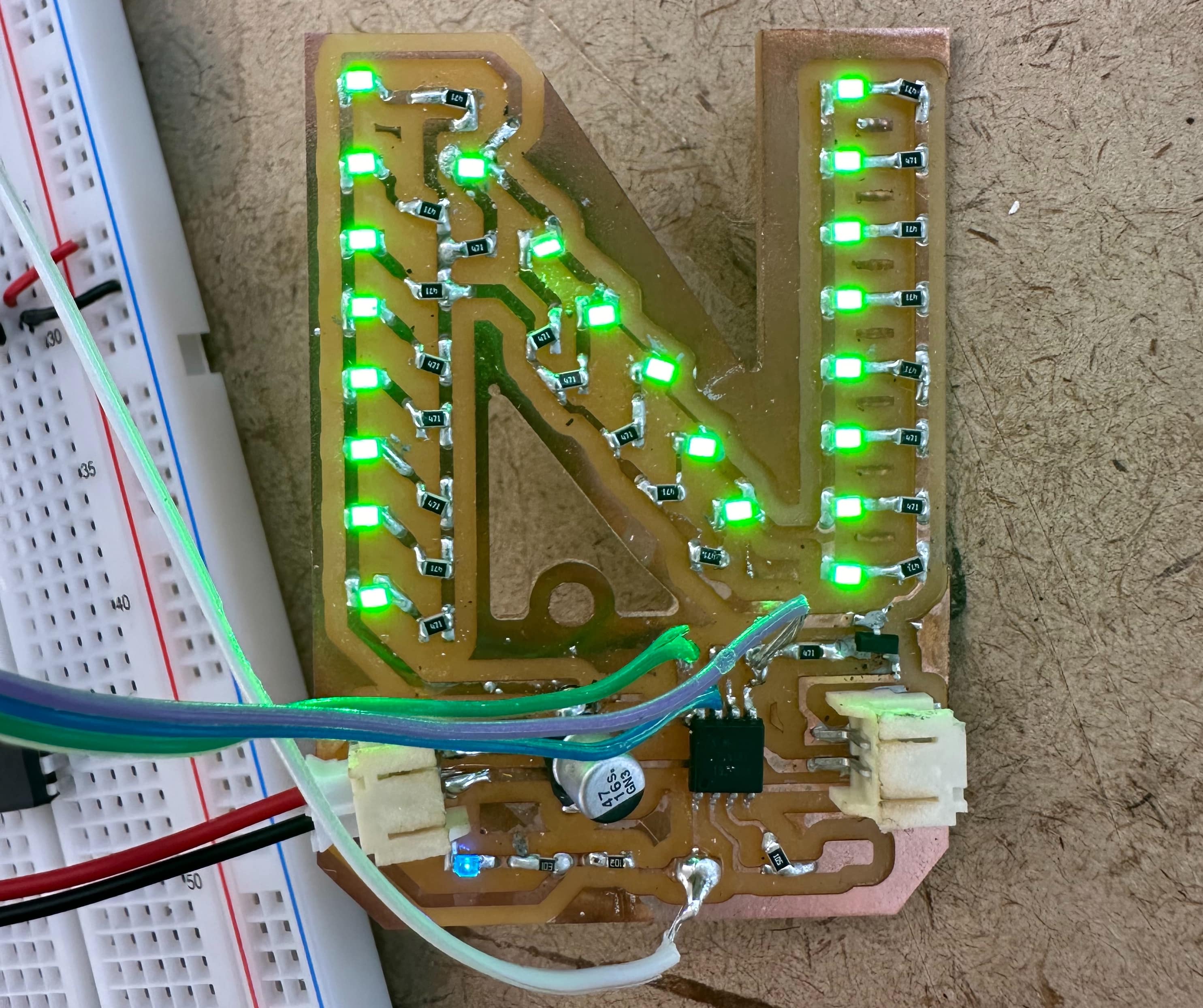 All 22 LEDs turning on!
Touch sensor setup
Almost there! The last problem was my capacitive touch sensor wasn't affecting the lights. The board was supposed to be interactive, so that when someone touches the conductive surface of the touch sensor the lights flash in a different pattern. The touch sensor is a small copper pad at the bottom right of my board, which feeds into the ATTiny input pins. Some code initializes this sensor and controls the LEDs based on sensor readings. There were a few things wrong here
- I mixed up the ATTiny pin numbers in my code. Each pin has multiple names: analog pin number, digital pin number, physical pin number. I needed to use digital pin numbers but I used the wrong ones, so my code was looking for the sensor at the wrong location and couldn't find it
- I was testing the capacitive touch sensor behavior by touching my finger to the bare copper on the board. I needed to solder a wire coming off of this so the sensor could get a more accurate, isolated reading After fixing these problems I had a fully functional board!
Touching the capacitive touch sensor to make the LEDs flash faster
I'm learned so much from taking this board from a design to a functional demo, and I'm excited to start designing my final project to continue DJELLO!